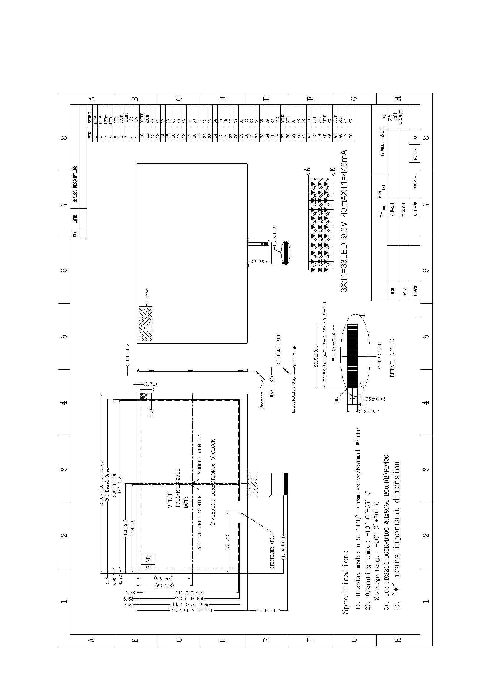
9 Inch High Definition Custom LCD Display Module
Model Number :
YY090IAF35WS300B1Display Size :
9 inch (Diagonal)Brightness :
300cd/m2Resolution :
1024*600Thickness :
3.5 MMDriver Element :
a-Si TFT active matrixWarranty :
12 MonthsManufacturer :
CloudSense OptiTechI: input,O: output,P: Powor
Note 1: DE/SYNC mode select. Normally pull high.
When select DE mode, MODE=”1”, VS and HS must pull high.
Whon solect SYNC mode, MODE=”0”, DE must be grounded.
Note 2: When input 18 bits RGB data, tho two low bits of R,G and B data must be grounded.
Note 3: Data shall be latched at the falling edge of DCLK.
Note 4: Selection of scanning mode
Note 5: Definition of scanning direction.
Refer to the figure as below:
Note 6: Global reset pin. Active low to enter reset state. Suggest to connect with an RC reset circuit for stability. Normally pull high.
Note 7: Dithering function enable control, normally pull high.
When DITHB=”1”,Disable internal dithering function,
When DITHB=”0”,Enable internal dithering function,
Note 8: Reserve for LED power input.
|
Pin No.
|
Symbol
|
I/O
|
Function
|
Remark
|
|
1
|
LED+
|
P
|
Power for LED backlight (Anode)
|
Note 8
|
|
2
|
LED+
|
P
|
Power for LED backlight (Anode)
|
Note 8
|
|
3
|
LED-
|
P
|
Power for LED backlight (Cathode)
|
Note 8
|
|
4
|
LED-
|
P
|
Power for LED backlight (Cathode)
|
Note 8
|
|
5
|
GND
|
P
|
Power ground
|
|
|
6
|
VCOM
|
I
|
Common voltage
|
|
|
7
|
DVDD
|
P
|
Power for Digital Circuit
|
|
|
8
|
MODE
|
I
|
DE/SYNC mode select
|
Note 1
|
|
9
|
DE
|
I
|
Data Input Enable
|
|
|
10
|
VS
|
I
|
Vertical sync input
|
|
|
11
|
HS
|
I
|
Horizontal sync input
|
|
|
12
|
B7
|
I
|
Blue data(MSB)
|
|
|
13
|
B6
|
I
|
Blue data
|
|
|
14
|
B5
|
I
|
Blue data
|
|
|
15
|
B4
|
I
|
Blue data
|
|
|
16
|
B3
|
I
|
Blue data
|
|
|
17
|
B2
|
I
|
Blue data
|
|
|
18
|
B1
|
I
|
Blue data
|
Note 2
|
|
19
|
B0
|
I
|
Blue data(LSB)
|
Note 2
|
|
20
|
G7
|
I
|
Green data(MSB)
|
|
|
21
|
G6
|
I
|
Green data
|
|
|
22
|
G5
|
I
|
Green data
|
|
|
23
|
G4
|
I
|
Green data
|
|
|
24
|
G3
|
I
|
Green data
|
|
|
25
|
G2
|
I
|
Green data
|
|
|
26
|
G1
|
I
|
Green data
|
|
|
27
|
G0
|
I
|
Green data(LSB)
|
Note 2
|
|
28
|
R7
|
I
|
Red data(MSB)
|
Note 2
|
|
29
|
R6
|
I
|
Red data
|
|
|
30
|
R5
|
I
|
Red data
|
|
|
31
|
R4
|
I
|
Red data
|
|
|
32
|
R3
|
I
|
Red data
|
|
|
33
|
R2
|
I
|
Red data
|
|
|
34
|
R1
|
I
|
Red data
|
Note 2
|
|
35
|
R0
|
I
|
Red data(LSB)
|
Note 2
|
|
36
|
GND
|
P
|
Power Ground
|
|
|
37
|
DCLK
|
I
|
Clock input
|
Note 3
|
|
38
|
GND
|
P
|
Power Ground
|
|
|
39
|
L/R
|
I
|
Left /right selection
|
Note 4,5
|
|
40
|
U/D
|
I
|
Up/down selection
|
Note 4,5
|
|
41
|
VGH
|
P
|
Gate ON Voltage
|
|
|
42
|
VGL
|
P
|
Gate OFF Voltage
|
|
|
43
|
AVDD
|
P
|
Power for Analog Circuit
|
|
|
44
|
RESET
|
I
|
Global reset pin.
|
Note 6
|
|
45
|
NC
|
-
|
No connection
|
|
|
46
|
VCOM
|
I
|
Common Voltage
|
Note 7
|
|
47
|
DITHB
|
I
|
Dithering function
|
|
|
48
|
GND
|
P
|
Power Ground
|
|
|
49
|
NC
|
-
|
No connoction
|
|
|
50
|
NC
|
-
|
No connection
|
|
